
Summary
The HV5122 (Microchip, DS20005418B) is a 32-channel serial-to-parallel converter with open-drain outputs — built for nixie tubes, VFDs, AC-EL displays, anything needing a lot of independently switched high-voltage sink channels from a simple 3-wire serial interface.
This isn't a "here's a schematic, trust me" post. Every component below has the actual reasoning attached — including one number I got wrong on the first pass and had to walk back once I did the arithmetic properly. That correction is left in on purpose; it's a better demonstration of the process than a clean answer would be.
::: tip Scope
Driver block only — logic decoupling, output protection, safe power-up. Not the HV
supply, not the MCU side, not the load. Full schematic + this write-up's reasoning
should be enough to adapt the values to your own load.
:::
Why this chip needs a protection design at all
The datasheet is explicit about this, and it's the reason this post exists instead of being three wires and a "done":
HV5122 / HV5222 are designed to be used in systems which either switch off the high voltage supply before changing the state of the high voltage outputs or which limit the current through each output.
Translation: there is no internal per-channel current limiting. Each HVOUT is an open-drain N-channel structure rated for a 100mA minimum sink. The only protection baked into the silicon is a clamp diode to GND at roughly -1.5V, which handles negative ringing on the output and does nothing at all for overcurrent. If you drive a load capable of sourcing more than the rated sink current — or you power-cycle the HV rail while an output's state is undefined — the die's survival depends entirely on circuitry you put around it. That's the brief for every choice below.
Pinout (subset used here)
44-pin PQFP (HV5122PG-G). Full pin table is in the datasheet; these are the ones this schematic wires up:
| Pin | Name | Function |
|---|---|---|
| 31 | VDD | Logic supply, 10.8–13.2V (typ 12V) |
| 30 | GND | Logic and HV ground — shared, no separate analog/power split on this part |
| 28 | OE | Output enable. LOW = all outputs forced off, regardless of shift register contents |
| 29 | CLK | Shift register clock, rising-edge |
| 32 | STR | Strobe — latches shifted data to outputs |
| 33 | DATA IN | Serial in |
| 23 | DATA OUT | Serial out, for cascading a second HV5122 |
| 35–38, ... | HVOUT1–4 (of 32) | Open-drain HV sink outputs, to 225V |
Schematic
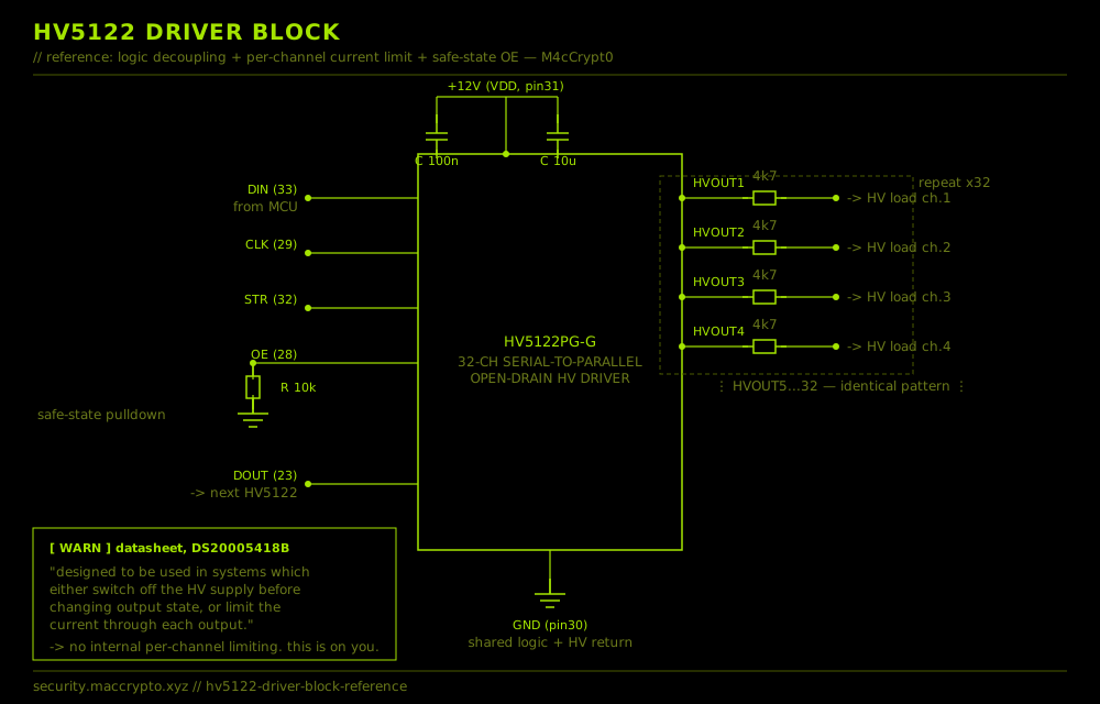
Custom-drawn symbol — Microchip doesn't publish a KiCad library for this part — with pin numbers matching the datasheet exactly for every pin used. DIN/CLK/STR/DATA OUT are left as unterminated stubs on purpose: that's the block's external interface to whatever's driving it (MCU direct, or a chain of these ICs).
The choices, and the actual numbers behind them
VDD decoupling — 100nF + 10µF, not just one cap
Two capacitors doing two different jobs, not redundancy:
- 100nF ceramic, right at the pin. The shift register clocks at up to 8MHz. A capacitor's usefulness at high frequency is bounded by its own parasitic inductance (ESL), and physically small ceramic packages have far lower ESL than anything electrolytic or tantalum — so this is the component actually suppressing clock-edge noise on VDD. Placement matters as much as the value: this one wants to be the closest thing to the pin, trace length adding inductance that partially defeats the point.
- 10µF bulk, alongside it. IDD is spec'd at 15mA max — modest on its own — but that's a steady-state clocking figure, not the current pulled the instant STR latches all 32 outputs simultaneously. The bulk cap is local charge storage for that transient so it doesn't have to be sourced through however much trace/wire inductance sits between this board and the main 12V rail.
Both ceramic, both rated well above 12V working voltage (25V+ parts, standard practice for margin against ripple and the DC-bias capacitance derating ceramics are prone to).
Per-channel series resistor — this is the "limit the current" requirement
This is the part I want to walk through properly, because my first pass at this value (2.2kΩ) doesn't survive the arithmetic and I want the correction on the record rather than quietly fixed.
The resistor's job: bound worst-case fault current through a channel to something the part survives, on the assumption that this resistor might be the only current limiting between the 200V rail and the HVOUT pin (worst case — a load fault, or a design where nothing else in the load path limits current).
I_fault = V_rail / RAt a 200V rail against the 100mA minimum sink rating:
| R | Worst-case fault current | Margin vs. 100mA rating |
|---|---|---|
| 1.0kΩ | 200mA | -100% (exceeds rating) |
| 2.2kΩ | 90.9mA | 9.1% |
| 3.3kΩ | 60.6mA | 39.4% |
| 4.7kΩ | 42.6mA | 57.4% |
| 6.8kΩ | 29.4mA | 70.6% |
| 10kΩ | 20.0mA | 80.0% |
2.2kΩ — my original number — leaves 9% margin against the rated minimum. That's not a safety margin, that's rounding error. It only makes sense as a value if you're also relying on something else downstream to share the current-limiting job (a ballast resistor already in the load's own circuit, or the load's own dynamic impedance during conduction) — and if that's true, say so explicitly rather than let the resistor value imply a safety margin that isn't really there.
::: warn Load current, separately
This table is about fault current — what happens if the load path collapses to
near-zero impedance. It says nothing about normal operating current or the
voltage this resistor eats out of your HV budget at that current (at 4.7kΩ and, say,
2.5mA nominal load current, that's ~11.75V dropped across the resistor — noticeable
on a 200V rail, not enormous). Size against both numbers, not just one.
:::
4.7kΩ is the default in this schematic — 57% margin, a reasonable middle ground when you don't know what's downstream. If your load already current-limits independently, you can go lower and get less voltage overhead eaten; if this resistor really is the only thing standing between the rail and the die, go higher. The formula's right there — recompute it for your actual rail voltage and load current rather than copying the number.
OE pull-down — 10kΩ, and why that specific value survives the leakage spec
On MCU reset or boot, GPIOs commonly default to high-impedance (floating) before
firmware configures them. A floating OE can read as an undefined logic level during
that window — and if the shift register happens to hold stale "on" data from before
the reset, every channel with a 1 in it fires the instant OE reads high. The
pull-down forces a known, safe default (all outputs off) regardless of what the MCU
is doing or how long it takes to get there.
The value has to satisfy two constraints simultaneously:
- Strong enough to hold the pin solidly low against the input's own leakage
current. HV5122's spec:
I_ILmax 1µA. At 10kΩ, that leakage produces1µA × 10kΩ = 10mV— three orders of magnitude below the ~2.0VV_ILthreshold. Effectively zero risk of leakage current pulling the "off" state out of spec. - Weak enough to not fight an actively-driven MCU output. A GPIO driving high presents an output impedance in the tens of ohms; 10kΩ is roughly 100–1000× higher, so the pull-down loses that fight instantly and costs negligible current (12V / 10kΩ ≈ 1.2mA when the MCU actively drives OE high — small, not worth optimizing further).
10kΩ sits comfortably in the middle of both constraints with margin on either side — no real motivation to deviate from it here, unlike the series-resistor case above where the "obvious" first value didn't actually hold up.
Power-up sequencing — a system requirement, not a pin
The datasheet's power-up sequence: connect ground, apply VDD, set all inputs to a known state — before anything downstream depends on output state being meaningful. This part has no dedicated HV supply pin (open-drain outputs sink current through whatever the external load ties them to), so "sequencing" here isn't something you wire on this chip — it's a requirement on whatever circuit enables your HV rail. Concretely: OE pull-down active (outputs forced off) and the shift register clocked to a known pattern, then — not before — let the external HV supply's enable go active. Getting this backwards is exactly the failure mode the OE pull-down above is defending against, from the other direction: known-safe logic state racing an HV rail that comes up on its own schedule.
::: danger Only 4 of 32 channels drawn
Channels 5–32 repeat the HVOUT1–4 pattern exactly — same resistor value, same
topology, same reasoning. Drawn as 4 + a dashed "repeat" boundary rather than all
32, because drawing all 32 would add scroll length and exactly zero additional
information.
:::
Lessons
- "Open-drain, current-sinking" on an HV driver puts the datasheet's stated protection requirement entirely on the board around it, not the silicon. Read "recommended operating conditions," not just the pinout table.
- A resistor value that "looks reasonable" and a resistor value that survives
I = V/Ragainst the actual worst-case rail voltage are not automatically the same number — 2.2kΩ felt fine until the arithmetic said 9% margin. Compute the fault case explicitly; don't eyeball it against a datasheet's typical-application table from a different voltage domain. - A pull-down sized against the input leakage spec (not just "10k is a normal pull-down value") is the difference between a value you can defend and a value that happens to work. Same effort either way — only one of them survives being asked "why that number."
- Sequencing (GND → logic supply → known logic state → then HV) is a system-level requirement here, not a per-chip one. Easy to satisfy by accident on a bench supply, easy to violate the first time someone adds a soft-start or an enable-on-boot HV converter to the same board.